A visit to Samsung’s massive new semiconductor hub
Samsung’s new Pyeongtaek semiconductor hub is scaling up massive fabs to meet the AI‑driven memory boom, reshaping the local workforce and the company’s market position.
Introduction
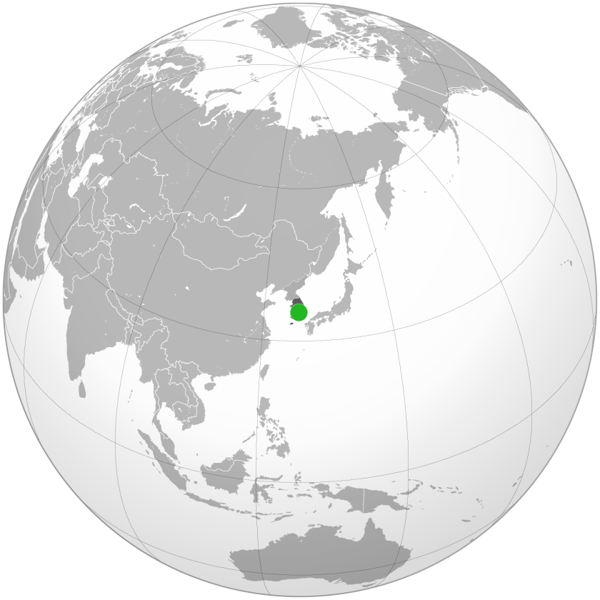
Samsung Electronics is expanding its semiconductor footprint in Pyeongtaek, South Korea, with a sprawling complex that now houses three operational fabs and a fourth ready to start production. A fifth fab, paused during a 2024 dip in memory demand, has been revived as generative AI fuels a surge in high‑bandwidth memory (HBM) needs. The site, roughly the size of New York’s Central Park, is becoming a focal point for the AI memory boom and a showcase of Samsung’s safety culture and labor dynamics.
Building the AI Memory Engine
Generative AI models rely on GPUs that, in turn, depend on stacks of specialized memory chips. Samsung’s new fabs are designed to produce the HBM chips that power these accelerators, aiming to reclaim market share from rivals such as SK Hynix and to compete with Taiwan’s TSMC in the broader foundry arena. Company forecasts predict sustained growth in memory demand through 2028, prompting the rapid construction of additional clean‑room capacity.
Life on the Factory Floor
The Pyeongtaek campus is a bustling micro‑city. Workers in black uniforms and sky‑blue vests stream out of the fabs for lunch, navigating a network of scooters, shuttle buses, and on‑site eateries. Safety officer Choi Hye‑rin, a 35‑year‑old overseeing cable‑duct crews, exemplifies the site’s emphasis on occupational health. Her daily routine includes helmet checks, chemical inspections, and spotter coordination for heavy equipment. The campus is dotted with safety slogans, LED scoreboards announcing poetry contests, and pledges on helmets that read, “I will not work if it’s not safe.”
Economic and Social Impact
The construction boom has turned Pyeongtaek—traditionally a farming community—into a high‑tech hub. Real‑estate offices line the perimeter, offering short‑term leases for studio apartments to accommodate the influx of engineers and laborers. Workers like Hye‑rin earn roughly 140,000 won (about $97) per day, a rate described as higher than typical construction sites, encouraging long‑term employment despite the demanding environment.
Looking Ahead
Samsung’s aggressive expansion reflects a strategic bet that AI‑driven workloads will keep memory demand elevated for years to come. By scaling production capacity and reinforcing safety protocols, the company aims to secure its position in the global memory market while fostering a sustainable workforce ecosystem in Pyeongtaek. The ongoing development of the fifth fab signals confidence that the AI memory surge is more than a temporary spike—it is reshaping the semiconductor landscape.
--- This article synthesizes observations from a recent visit to Samsung’s Pyeongtaek semiconductor hub, highlighting the site’s operational scale, safety culture, and its role in the broader AI memory supply chain.
Source
Read original sourceWhy we picked this
Discusses semiconductor manufacturing crucial for generative AI hardware.